


Key Advantages of HDI PCBs
HDI PCBs are especially cost-effective when the layer count exceeds 8, and they offer superior performance compared to traditional multilayer PCBs in high-density applications. Their benefits include:
-
💰 Reduced cost for high-layer designs
-
📐 Higher wiring density, allowing smaller board sizes
-
⚡ Improved electrical performance and signal integrity
-
🔒 Enhanced reliability through optimized via structures
-
🔥 Better thermal management
-
📡 Superior EMI/ESD/RFI control
-
🧠 Increased design flexibility and efficiency
As electronics evolve toward miniaturization and precision, HDI technology becomes essential in delivering compact form factors without compromising performance.
Applications of HDI PCBs
HDI boards are widely adopted in industries that demand small size, high performance, and dense component integration, including:
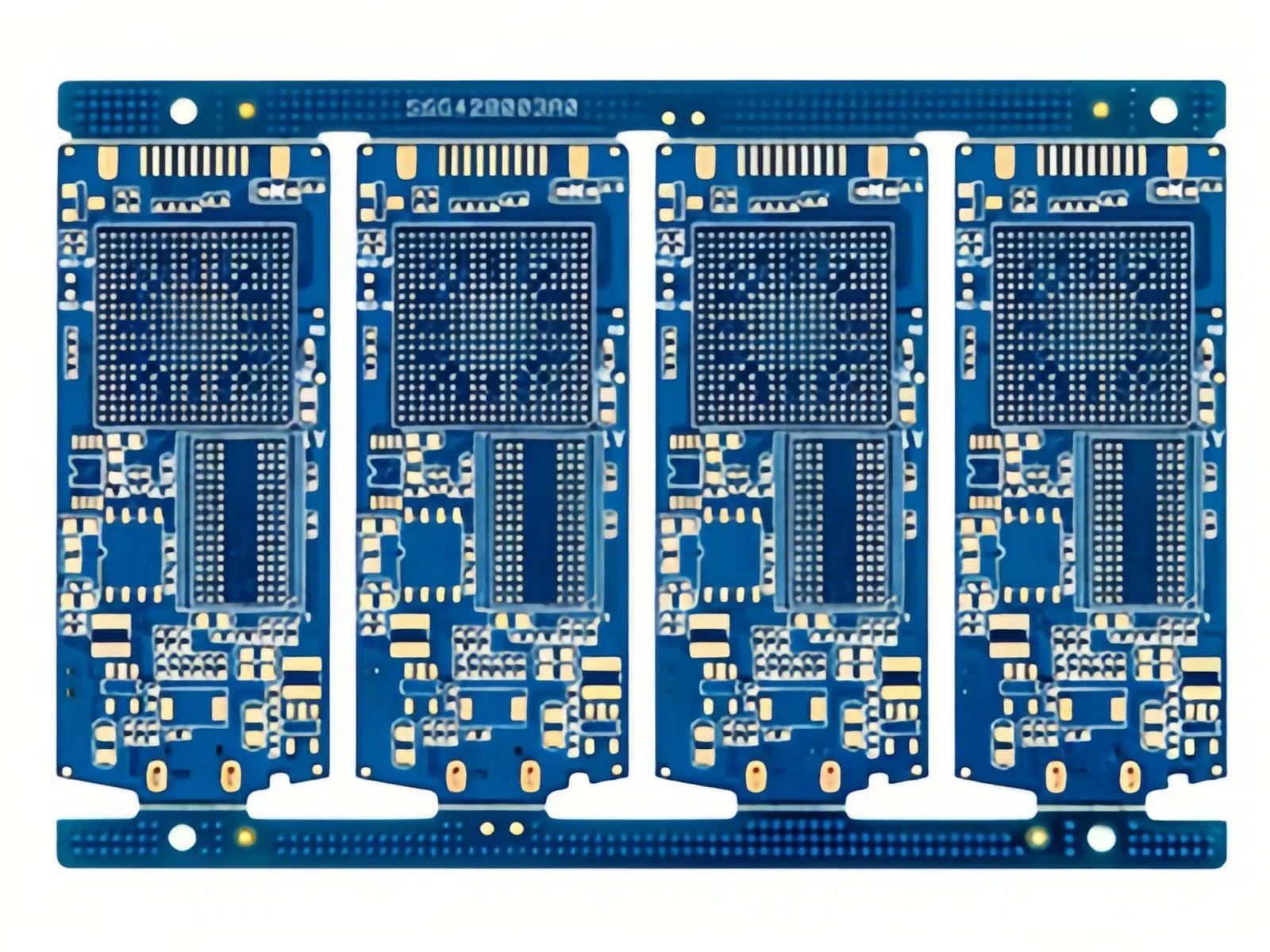
Consumer Electronics
HDI PCBs enable compact, lightweight devices such as:
-
Smartphones (largest demand)
-
Digital cameras (DSLRs, action cams)
-
MP3/MP4 players
-
Laptops and tablets
-
Wearables and handhelds
Automotive & Aerospace
Used in lightweight control units, advanced driver-assistance systems (ADAS), flight controllers, and other space-constrained electronics.
Medical Devices
One of the fastest-growing HDI application areas:
-
Enables miniaturized diagnostic tools and implants
-
Supports low power, high-speed signal transmission, and mechanical compatibility with human anatomy
-
Delivers stable performance in mission-critical environments
Why Choose HDI for Your Project?
HDI technology offers the ideal balance of performance, size, cost, and reliability, making it indispensable in today’s high-end PCB designs. Whether you’re building consumer gadgets, automotive control systems, or cutting-edge medical devices, HDI PCBs are your path to smarter, smaller, and more efficient electronic solutions.
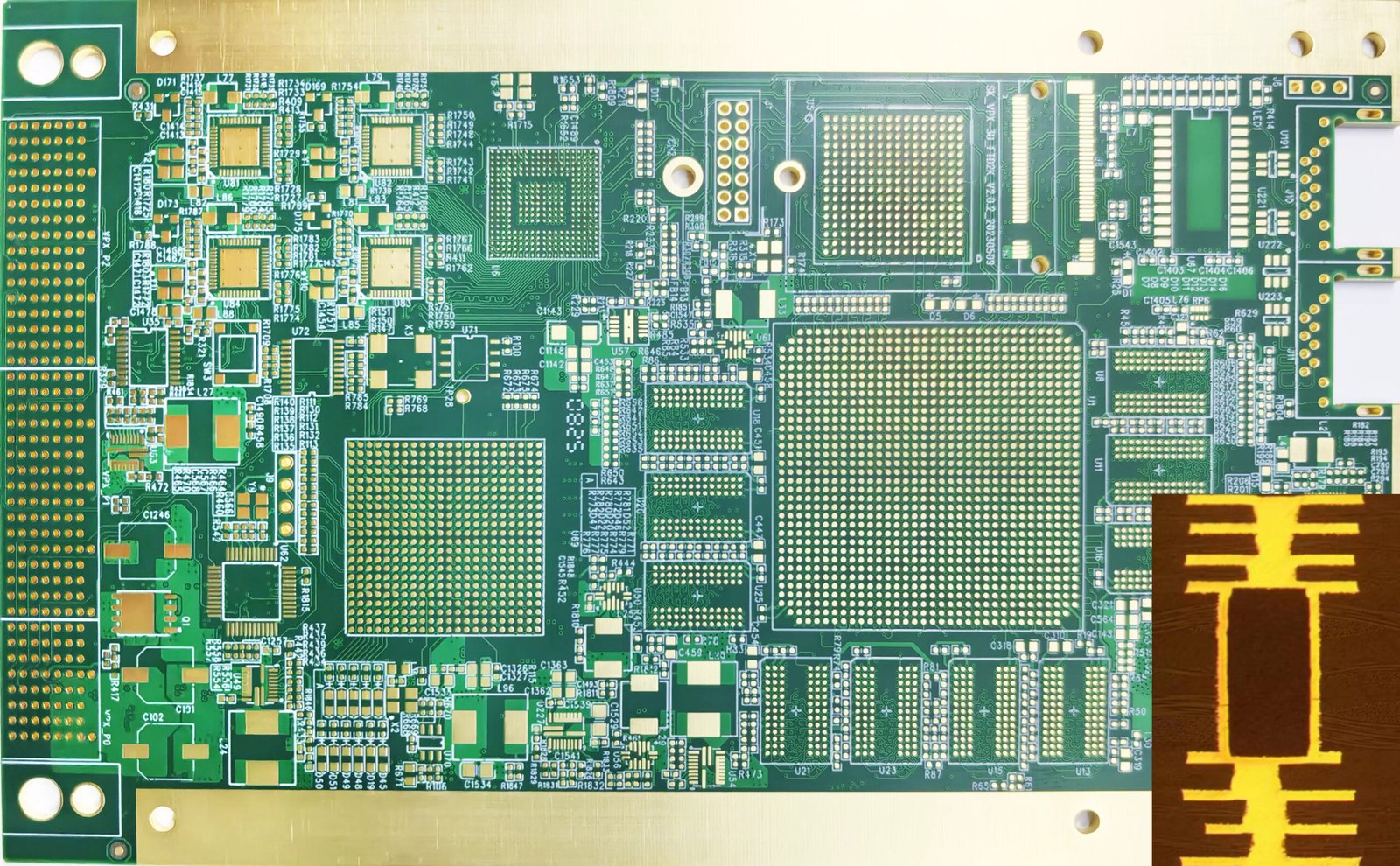
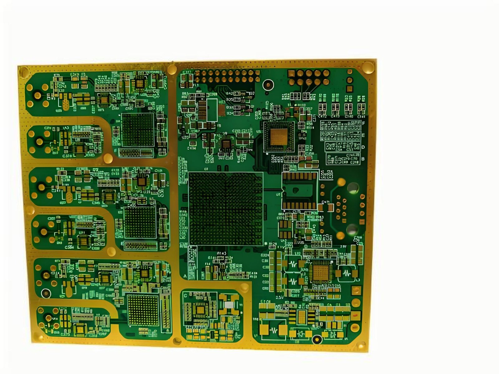
Technical Specifications
| Number of Layers | 4 – 16 layers (standard), up to 22 layers (advanced) |
| Technology Highlights | High-density interconnect boards with finer lines/spaces, smaller vias and capture pads, and micro-vias in pads that only penetrate specific layers |
| HDI Builds | 3+N+3, 4+N+4, Any-layer HDI in R&D |
| Materials | FR4 (standard & high performance) Halogen-free FR4 Rogers |
| Finished Copper Weights | 18 μm – 70 μm |
| Minimum Track / Gap | 0.075 mm / 0.075 mm |
| PCB Thickness | 0.40 mm – 3.20 mm |
| Maximum Dimensions | 610 mm × 450 mm (depends on laser drilling machine) |
| Surface Finishes | OSP ENIG Immersion Tin Immersion Silver Electrolytic Gold Gold Fingers |
| Minimum Mechanical Drill | 0.15 mm |
| Minimum Laser Drill | 0.10 mm (standard), 0.075 mm (advanced) |