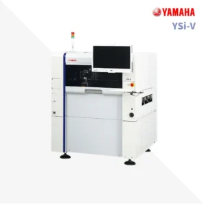
Outstanding Products Make You Stand Out
Each SMT pick and place machine is guaranteed to boost your PCB assembly business thanks to the number of qualities listed below.
- ⚡Precise Placement: The accuracy of our SMT pick and place machines can achieve a level of precision that surpasses any human pick and place handling.
- 🔥High Flexibility: All SMT pick and place machines are easy to program for various PCB boards with different dimensions, production requirements, and specifications.
- 🧱Ease of Use: With the user-friendly aspect of our SMT pick and place machines, they can be incorporated into your production floor with the minimum training requirement.
- 🧩Low Maintenance: The cutting-edge technology of our SMT pick and place machines requires minimal maintenance, helping you reduce cost while increasing productivity.
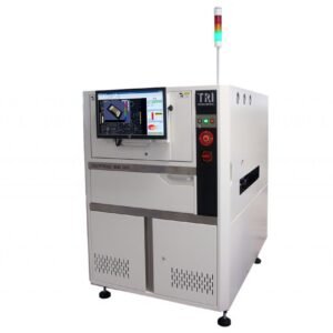
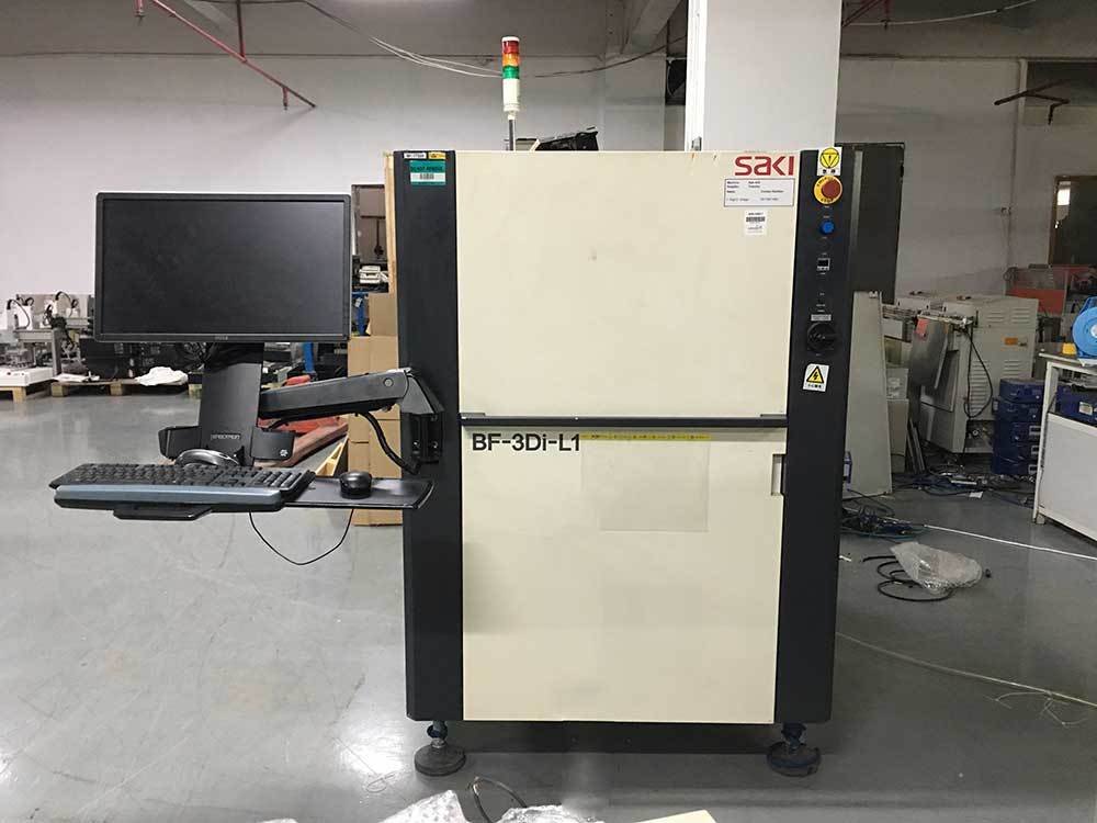
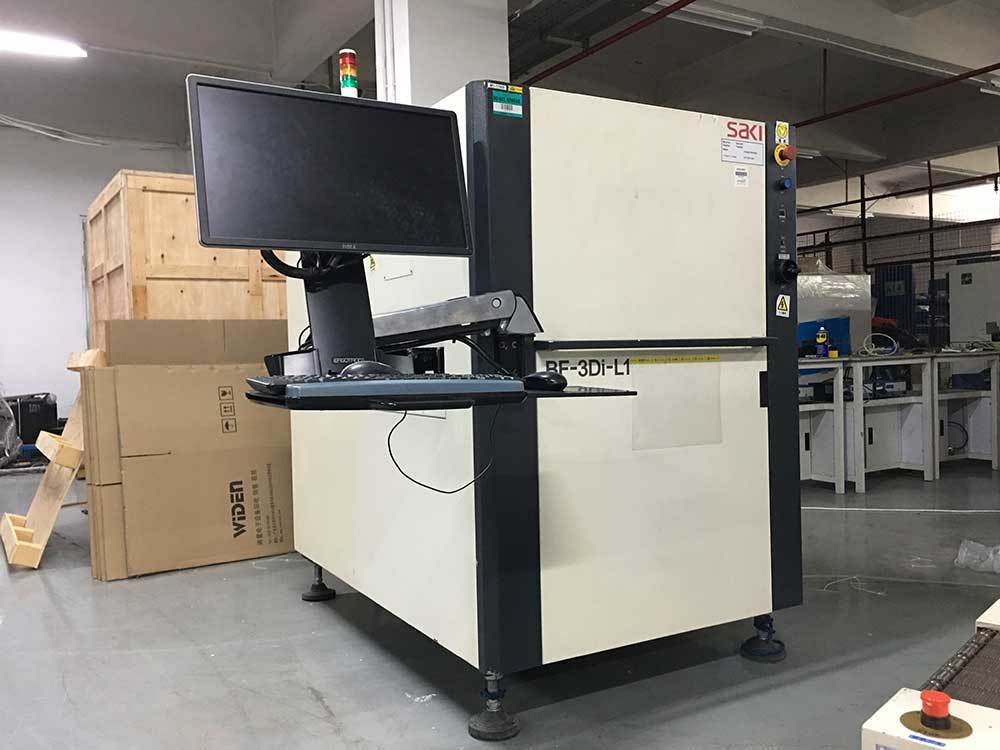
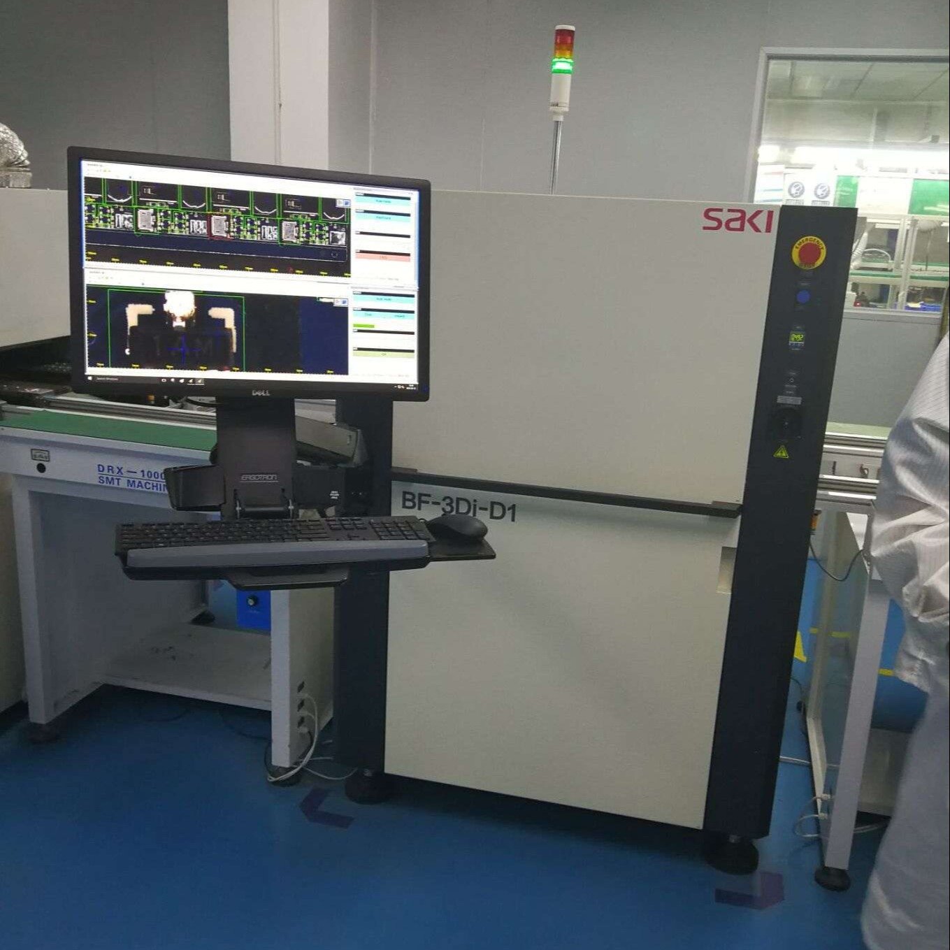
🔶 SAKI BF-3Di-L1 3D Automated Optical Inspection Machine Specifications
| Model | BF-3Di-L1, BF-3Di-Z1 | ||
| Design Reference Provision | Machinery Directive Annex-I, EN ISO12100, EN ISO13849-1, EN60204-1, EN ISO13857 | ||
| Dimensions | 1040 (W) x 1530 (D) x 1500 (H) mm (BF-3Di-L1) | ||
| (40.94 W x 60.24 D x 59.06 H in.) | |||
| 1340 (W) x 1530 (D) x 1500 (H) mm (BF-3Di-Z1) | |||
| (52.75 W x 60.24 D x 59.06 H in.) | |||
| Maintenance Space | 1m in front of the machine, 1m in rear of the machine, 1m in side of the machine | ||
| Weight | Approx. 950 kg (2094.39 lb) | ||
| Usage Environment | Temperature: 15 to 30 degree C, Humidity: 15 to 80 %RH (Non Condensing), Height above Sea Level under: 0 to 1000 m, Overvoltage Category : (IEC60664-1), Pollution Degree : 2 (IEC60664-1) | ||
| Transport Environment | Temperature: 15 to 30 degree C, Humidity: 15 to 80 %RH (Non Condensing) | ||
| Operating Environment | Single phase, 200 to 240V ±10%, 50/60Hz, 700VA | ||
| Noise Level | 68 dB(A), Operating Condition: Full load, Measuring Method: According to clause 1.7.4.2 of Machinery Directive 2006/42/EC | ||
| Air Requirement | 0.5 MPa @ ≥ 5 L/min (ANR) | ||
| Target PCB | PCB Size | 50 (W) x 60 (L) – 460 (W) x 510 (L) mm (BF-3Di-L1) | |
| (1.97 W x 2.36 L to 18.11 W x 20.07 L in.) | |||
| 50 (W) x 60 (L) – 686 (W) x 870 (L) mm (BF-3Di-Z1) | |||
| (1.97 W x 2.36 L to 27.00 W x 34.25 L in.) | |||
| PCB Thickness | 0.6 to 5.2 mm (0.02 to 0.204 in.) (*2) | ||
| PCB Weight | 6 kg (13.2 lb) or less (BF-3Di-L1) | ||
| 8 kg (17.6 lb) or less (BF-3Di-Z1) | |||
| Material | Glass Epoxy, Paper Phenol, Ceramic | ||
| Warpage | 2 mm (0.08 in.) or less | ||
| PCB Clearance (Top) | 40 mm (1.57 in.) (*3) | ||
| PCB Clearance (Bottom) | 40 mm (1.57 in.) | ||
| Fiducial Mark | One mark at any corner and another at the opposing corner (total two marks and above) | ||
| Transfer Conveyor | Height | 880 to 965 mm (34.65 to 37.99 in.) | |
| Method | Flat belt transfer | ||
| Width Adjustment | Auto | ||
| PCB Setting | Clamp at contact-stopper and rail transfer width. Clamp width is 3 mm-wide (0.12 in.-wide) at each side. |
||
| Transfer Direction | Left to Right / Right to Left | ||
| Machine Origin | Front | ||
| Detect the Position of the Stopper Sensor | Detect the (Rail width) x 0.4 position from front rail | ||
| Optical System | Lighting | 2D | CoaxialtopLight: Red LED |
| TopLight: Red LED | |||
| SideLight: Blue LED (First Line), Green LED (Second Line), Red LED (Third Line) | |||
| LowLight: Red LED | |||
| 3D | White LED (with the stripe pattern projection function) (*4) | ||
| Camera | CMOS area camera | ||
| Resolution | 18 μm | ||
| Imaging | FOV camera gantry (*5) | ||
| FOV Size | 36 (W) x 36 (L) mm (1.417 W x 1.417 L in.) | ||
| Communication Feature | Network I/F | Ethernet (1000BASE-T) | |
| Signal Tower | Red, Yellow, Green from above | ||
| Signal Interface | Upstream Machine | READY signal (Dry contact), BUSY signal, OK/NG signal | |
| Downstream Machine | READY signal, BUSY signal (Dry contact), OK/NG signal (Dry contact) | ||
| Inspectable Components | 0402 mm (01005 in.) packages and up, Diodes, Tantalum capacitors, Aluminum electrolytic capacitors, Module chips, Transistors, Power transistors, MELF resistors, Filters, Special shaped components, Connectors (0.4 mm pitch and up), QFP, SOP, CSP, BGA (0.4 mm pitch and up), and Solder joints viewable from vertical top (*1) | ||
| Inspection Categories | Presence/Absence, Misalignment, Tombstone, Reverse, Polarity, Bridge, Absence of solder, Insufficient solder, Lifted lead, Lifted chip, and Fillet defect. Each defect name can be arranged freely by system function (*2) | ||
| Inspection Method | Inspections are processed after capturing each FOV. Height differences are detected by projecting stripe patterns from maximum four directions. | ||
| Inspection Image | Images taken by different angle lightings (CoaxialtopLight, TopLight, SideLight, LowLight), color images taken by SideLight, visualized height information, and composite of those images. | ||
| Data Import | CAD data, Mount Data, or NC data | ||
| Fiducial Mark | Shape | Circle, Square, Triangle, Rhomboid | |
| Offset Calculation | Two-point, Three-point | ||
| Tact Time | Tact time is calculated by adding image capturing time and PCB loading/unloading time. (*3) (*4) | ||
| Image Capturing Time | 0.39 sec./FOV (approximately 2.5 FOV/sec.) | ||
| PCB Loading/ Unloading Time | Approximately 5 sec. | ||
| Measurable Height | 20 mm (0.79 in.) or less | ||
| Measurement Accuracy | Height Resolution 1 μm Height Inspection Repeatability 2 μm (3) or less (*5) |
||
| Inspection Result Output | Screen display of defect locations, File output of defect details, Image output of defective area, and Network output of the above files | ||
| Recognizing Ability | OCR function, 1D barcode, 2D barcode | ||
| Note: (*1) J lead fillet for PLCC and BGA/CSP bottom solder joints are excluded from inspectable categories. Side camera(optional function) enables to inspect materials that cannot be seen from just above such as the solder fillet of J leads. (*2) Inspection categories are limited to items viewable on inspection images. (*3) Calculation and image capturing are processed at the same time. If the inspection data is heavier, the tact time becomes longer. (*4) Image Capturing time and PCB Loading/Unloading time are for reference purpose only. (*5) By using Saki’s Height calibration jig. When using 2500 μm height jig, repeatability is 2 μm (3σ) or less. When using 8000 μm height jig, repeatability is 10 μm (3σ) or less. |
|||
| Operating System | Microsoft Windows 10 IoT Enterprise 64bit English version | ||
| Inspection Software Language | English or Japanese | ||