


🔶 Advantages of Thick PCBs (Including Heavy Copper)
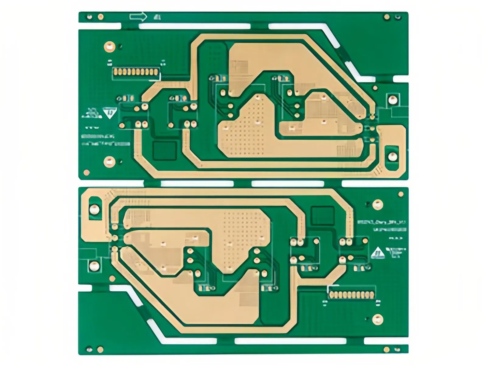
Thick PCBs refer to circuit boards with increased overall thickness — whether due to multilayer stacking, high copper weights, or structural demands. Compared to standard PCBs (typically ~1.6 mm thick with 35 μm copper), thick PCBs offer significantly improved power handling, thermal performance, and mechanical durability. Copper thicknesses often range from 70 μm (2 oz) to 140 μm (4 oz) or more, especially in heavy copper designs.
Key benefits include:
- ⚡ Higher current-carrying capacity
- 🔥 Improved heat resistance and dissipation
- 🧱 Enhanced mechanical strength of connectors and plated-through holes (PTH)
- 🧩 Reduced product size by eliminating the need for multiple parallel traces
- 🛡️ Excellent corrosion resistance, even in harsh environments
- ✅ Stable performance across wide temperature ranges
Thick copper layers also create a robust and non-toxic passivized surface, adding long-term reliability to the board.
🔶 Applications of Thick PCBs
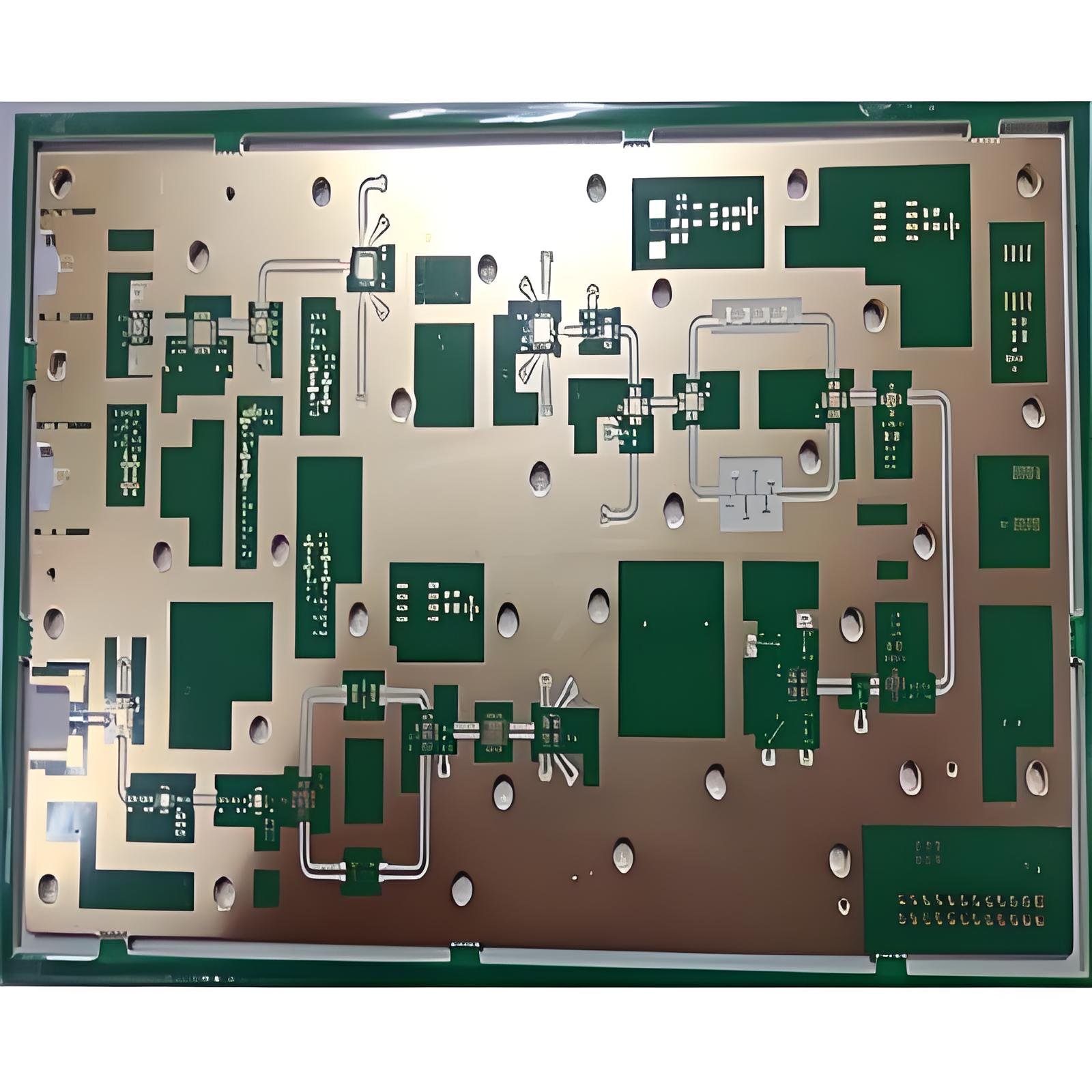
Thick PCBs are primarily used in high-current and power-conversion systems, where efficiency, thermal management, and structural integrity are critical. They are especially common in:
● Power Electronics
- Power modules
- Power supplies
- DC-DC converters
- Battery management systems (BMS)
● Automotive & EV Systems
- On-board chargers
- Motor control units (MCUs)
- Inverters
- LED drivers
● Industrial & Renewable Energy
- Solar power converters
- Wind turbine controllers
- Smart grid components
🔶 Market Trend
With the rapid expansion of electric vehicles (EVs) and high-power electronics, the demand for thick PCBs has surged. Boards with 6 oz copper or more are now widely adopted, enabling the safe conduction of high current and managing increasingly intense thermal loads.
As electronic systems evolve toward higher density, greater power, and smaller footprints, thick copper technology plays a vital role in delivering reliable, high-performance solutions.
🔶 Technical Specifications
| Quality Grade | IPC Class 2, IPC Class 3 |
| Number of Layers | 4 – 30 layers |
| Material | FR4 Tg140, High Tg FR4 Tg170 |
| Maximum Board Size | 450 mm × 600 mm |
| Final Board Thickness | 0.6 mm – 6.5 mm |
| Max Outer Layer Copper | 15 oz |
| Max Inner Layer Copper | 12 oz |
| Min. Track / Spacing – External | 9 mil / 11 mil (4 oz Cu) |
| Min. Track / Spacing – Internal | 8 mil / 12 mil (4 oz Cu) |
| Min. Hole Size | 10 mil (≈0.25 mm) |
| Solder Mask Color Options | Green, Matte Green, Yellow, White, Blue, Purple, Black, Matte Black, Red |
| Silkscreen Color Options | White, Black |
| Surface Treatments | HASL (Lead-free), ENIG, Immersion Silver, OSP, Hard Gold, ENEPIG |
| Testing Methods | AOI Test, Flying Probe Test |
| Lead Time | 2 – 28 days |
| Certifications | ISO 13485, TS 16949 |